CMOS (Complementary Metal Oxide Semiconductor)
The main advantage of CMOS over NMOS and BIPOLAR technology is the much smaller power dissipation. Unlike NMOS or BIPOLAR circuits, a Complementary MOS circuit has almost no static power dissipation. Power is only dissipated in case the circuit actually switches. This allows integrating more CMOS gates on an IC than in NMOS or bipolar technology, resulting in much better performance. Complementary Metal Oxide Semiconductor transistor consists P-channel MOS (PMOS) and N-channel MOS (NMOS).

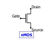
NMOS
NMOS is built on a p-type substrate with n-type source and drain diffused on it. In NMOS, the majority carriers are electrons. When a high voltage is applied to the gate, the NMOS will conduct. Similarly, when a low voltage is applied to the gate, NMOS will not conduct. NMOS are considered to be faster than PMOS, since the carriers in NMOS, which are electrons, travel twice as fast as the holes.
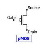
PMOS
P- channel MOSFET consists P-type Source and Drain diffused on an N-type substrate. Majority carriers are holes. When a high voltage is applied to the gate, the PMOS will not conduct. When a low voltage is applied to the gate, the PMOS will conduct. The PMOS devices are more immune to noise than NMOS devices.
CMOS Working Principle
In CMOS technology, both N-type and P-type transistors are used to design logic functions. The same signal which turns ON a transistor of one type is used to turn OFF a transistor of the other type. This characteristic allows the design of logic devices using only simple switches, without the need for a pull-up resistor.
In CMOS logic gates a collection of n-type MOSFETs is arranged in a pull-down network between the output and the low voltage power supply rail (Vss or quite often ground). Instead of the load resistor of NMOS logic gates, CMOS logic gates have a collection of p-type MOSFETs in a pull-up network between the output and the higher-voltage rail (often named Vdd).
Thus, if both a p-type and n-type transistor have their gates connected to the same input, the p-type MOSFET will be ON when the n-type MOSFET is OFF, and vice-versa. The networks are arranged such that one is ON and the other OFF for any input pattern as shown in the figure below.

CMOS offers relatively high speed, low power dissipation, high noise margins in both states, and will operate over a wide range of source and input voltages (provided the source voltage is fixed). Furthermore, for the better understanding of the Complementary Metal Oxide Semiconductor working principle, we need to discuss in brief about CMOS logic gates as explained below.
CMOS Inverter
The inverter circuit as shown in the figure below. It consists of PMOS and NMOS FET. The input A serves as the gate voltage for both transistors.

The NMOS transistor has an input from Vss (ground) and PMOS transistor has an input from Vdd. The terminal Y is output. When a high voltage (~ Vdd) is given at input terminal (A) of the inverter, the PMOS becomes open circuit and NMOS switched OFF so the output will be pulled down to Vss.
When a low-level voltage (<Vdd, ~0v) applied to the inverter, the NMOS switched OFF and PMOS switched ON. So the output becomes Vdd or the circuit is pulled up to Vdd.
| INPUT | LOGIC INPUT | OUTPUT | LOGIC OUTPUT |
| 0 v | 0 | Vdd | 1 |
| Vdd | 1 | 0 v | 0 |
CMOS NAND Gate
The below figure shows a 2-input Complementary MOS NAND gate. It consists of two series NMOS transistors between Y and Ground and two parallel PMOS transistors between Y and VDD.

If either input A or B is logic 0, at least one of the NMOS transistors will be OFF, breaking the path from Y to Ground. But at least one of the pMOS transistors will be ON, creating a path from Y to VDD.
Hence, the output Y will be high. If both inputs are high, both of the nMOS transistors will be ON and both of the pMOS transistors will be OFF. Hence, the output will be logic low. The truth table of NAND logic gate given in below table.
| A | B | Pull-Down Network | Pull-up Network | OUTPUT Y |
| 0 | 0 | OFF | ON | 1 |
| 0 | 1 | OFF | ON | 1 |
| 1 | 0 | OFF | ON | 1 |
| 1 | 1 | ON | OFF | 0 |
CMOS NOR Gate
A 2-input NOR gate is shown in the figure below. The NMOS transistors are in parallel to pull the output low when either input is high. The PMOS transistors are in series to pull the output high when both inputs are low, as given in below table. The output is never left floating.

The truth table of NOR logic gate given in below table.
| A | B | Y |
| 0 | 0 | 1 |
| 0 | 1 | 0 |
| 1 | 0 | 0 |
| 1 | 1 | 0 |
CMOS Applications
Complementary MOS processes were widely implemented and have fundamentally replaced NMOS and bipolar processes for nearly all digital logic applications. The CMOS technology has been used for the following digital IC designs.
- Computer memories, CPUs
- Microprocessor designs
- Flash memory chip designing
- Used to design application specific integrated circuits (ASICs)
Also watch EEE Projects


