Monday, 30 October 2023
Wireless device makes magnetism appear in non-magnetic materials
Friday, 27 October 2023
New research finds stress and strain changes metal electronic structure
Thursday, 26 October 2023
Controlling waves in magnets with superconductors for the first time
A superatomic semiconductor sets a speed record
Using sound to test devices, control qubits
Monday, 23 October 2023
Cathode active materials for lithium-ion batteries could be produced at low temperatures
Sunday, 22 October 2023
Researchers demonstrate a high-speed electrical readout method for graphene nanodevices
Friday, 20 October 2023
From square to cube: Hardware processing for AI goes 3D, boosting processing power
Thursday, 19 October 2023
Electrical control of quantum phenomenon could improve future electronic devices
Wednesday, 18 October 2023
From a five-layer graphene sandwich, a rare electronic state emerges
Thursday, 12 October 2023
Revolutionizing energy storage: Metal nanoclusters for stable lithium--sulfur batteries
Tuesday, 10 October 2023
Magnetoelectric material can reconnect severed nerves
Wireless, battery-free electronic 'stickers' gauge forces between touching objects
Bipolar Junction Transistor – A Getting Started Guide for Beginners
The Bipolar Junction Transistor (BJT) is one of the two most used types of transistors. You can use it to create audio amplifiers, switch on/off DC lamps, motors, and much more.
In this tutorial aimed at beginners, you’ll learn the basics you need to start having fun and design your own transistor circuits.

Introduction to Bipolar Junction Transistors
The Bipolar Junction Transistor (BJT) is a device made of three layers of semiconductor material; these layers can be either P-type or N-type. The pins of a BJT are named base, collector, and emitter. Each pin is connected to one of these layers.
There are two different types of BJTs known as PNP and NPN. They are named after the arrangement of the semiconductor layers. You can see the construction and symbols of PNP and NPN transistors below.

How the Bipolar Junction Transistor Works
The BJT has two operation modes. It can be used as:
- an amplifier, which means that it can magnify an input signal (for example audio)
- a switch that can turn things (motors, lights, etc) on or off
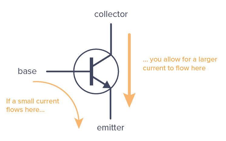
But, how can you select between one behavior and the other? It all depends on the current that flows through the base. So to be able to design transistor circuits, you need to start by learning how currents flow in a bipolar transistor.
A BJT is controlled by current. For an NPN transistor, a small current flowing into the base turns the transistor ON so that a bigger current can flow from collector to emitter.
β is the gain of your transistor that tells you how much bigger than the base current the collector current is.

This value is given by the manufacturer, and it’s also known as hFE. You’ll find it in the datasheet of the transistor.
The path from base to emitter works like a diode with a forward voltage of about 0.7V.
The emitter current (IE) equals the sum of the base current (IB) and the collector current (IC). This makes sense since the base and collector currents flow into the transistor, and there is nowhere else for the currents to flow than out from the emitter.
So you have:

The PNP transistor works the same way, just that the currents flow the opposite way.

Basic BJT Configurations
There are essentially three ways to connect a BJT in a circuit, and they are named based on which terminal serves as a common connection point for the input and the output. The three configurations are:
- Common-Emitter Configuration (The most common)
- Common-Collector Configuration (Mostly used for creating a buffer)
- Common-Base Configuration (Not that common)

Common Emitter
The common-emitter configuration is the most common way to connect a transistor circuit. It’s used both to connect the transistor as a switch and to use it as an amplifier. This setup is great for amplifying a tiny voltage or current into a much higher voltage on the output.
In the circuit below an NPN transistor is set up as a common emitter. Its base is connected to the input voltage via a resistor RB.
To simplify, the input voltage VBB is represented as a battery. But this is normally a signal such as an audio signal or a microcontroller output pin.

The collector is connected to the DC power source VCC through a resistor RL. RL can either be something you want to control (like a motor or a speaker), or it can be a resistor set to get a specific output voltage range from the collector terminal.
The emitter is connected to the negative terminals of both power supplies, hence the name common emitter.
Common Emitter Calculations
When you design a transistor circuit, you usually want to design it so that you have a specific current flowing through the load RL. For example, if RL is a motor, you want to make sure the motor gets enough current to turn on.
The current that flows through RL is the same as the collector current (IC) and you can find it from the value of IB with the following formula as discussed above:
To find the base current (IB), you need to find the current that flows through RB. You can find it from the input voltage (VBB) using the following formula:

VBE is always around 0.7V (given that the input voltage is high enough). So by adjusting the value of RB, you can set the base current, and thereby the collector current, to the value that you need.
Common Collector
The common-collector configuration is often used to create a voltage follower or buffer. The output voltage is the same as the input voltage minus 0.7V.
A buffer is useful if you have a signal source that can’t provide enough current for your load. With this circuit, it’s the transistor you choose that determines the maximum current, not the signal source.

When the transistor is turned on, the voltage drop from the base to the emitter is ~0.7V. So when you connect a bipolar-junction transistor in the common-collector configuration, you know that the output is always 0.7V lower than the input. So the output voltage follows the input voltage.
Common Base
The common-base configuration isn’t very common when building circuits with discrete components. However, it’s popular in integrated circuits and RF amplifiers for high frequency. You can learn more about the common-base configuration and how to set it up from this page.
Note: The operating principle for both PNP and NPN transistor types is identical; the only distinction lies in their biasing and the polarity of the power supply for each type.
Operating Regions of a Bipolar Junction Transistor
A transistor can be fully on, fully off, or somewhere in between. These are the operating regions of the bipolar junction transistor.
- Saturation Region (Transistor is turned fully ON)
- Cut-off Region (Transistor is turned OFF)
- Active Region (Transistor is somewhere between fully ON and OFF)
You can set your transistor into each of these regions by controlling the base current (IB):
If there is no base current, the transistor is off, so it’s in the cut-off region. As you start to increase the base current, the transistor goes into the active region, where it’s partially on. At some point, when the base current is high enough, the transistor goes into the saturation region where it turns fully on.
If you want to use the transistor as a switch, you want to have the transistor in the Cut-off region (open switch) or the Saturation region (closed switch).
If you want to use the transistor as an amplifier, it is the Active region you want to be in. In the active region, the collector current can be found from the base current and the gain (β):
The BJT Transistor as a Switch
To use a bipolar junction transistor as a switch, use the common emitter configuration:
- Emitter: Connected to the ground (0V reference).
- Collector: Connected to the load (e.g., a lamp).
- Base: Connected to the control signal (e.g., push button, microcontroller).
- Load: Connected between the collector and the supply voltage.

Switch Off (Cut-off Region)
To turn the switch off, you need to set the base current to zero which puts the transistor into its cut-off region. So you have:
- No Base current (IB = 0)
- Base-Emitter voltage VBE < 0.7v
- No Collector current ( IC = 0 )
- VCE = VCC
- The transistor operates as an open switch

Switch On (Saturation Region)
To turn the switch on, you need to have enough base current to place the transistor into the saturation region. So you have:
- Enough base current to place the transistor into saturation
- Base-Emitter voltage VBE > 0.7v
- VCE = 0 (ideally)
- Maximum collector current (IC = VCC/RLOAD)
- The transistor operates as a closed switch

Bipolar Junction Transistor as an Amplifier
If you want to use the BJT as an amplifier, the most common configuration is the common emitter.
Below is a simple amplifier circuit that drives a speaker. The voltage on the input decides the base current. So the higher the voltage, the higher the current.

The collector current (which is the same current that goes through the speaker) is limited to the gain of the transistor multiplied by the base current. The base current will vary with the input voltage, which means the collector current will also vary with the input voltage.
So a varying input voltage makes the current in the speaker vary, which creates sound.
To start having current flowing through the speaker in the above example, the input voltage must be around 0.7V as a minimum, since that’s the point where the transistor turns on. If the input voltage is below this, the transistor will be off.
And you can’t increase the current through the speaker more than what is dictated by VCC and the speaker resistance (IC(MAX) = VCC/RLOAD). So there is a certain voltage on the input that will be the max, and increasing it more won’t make a difference.
So you have a minimum and a maximum input voltage.
But what if the signal you want to amplify does not match that range?
This is where biasing comes in.
BJT Amplifier Biasing
By adding resistors, you can make sure your amplifier accepts a different range of input signals to match whatever you want to amplify. In technical terms, you are biasing the transistor to work in the active region.

R1 and R2 divide the VCC voltage and set the bias voltage for the base so that the transistor is in the active region. C1 and C3 are coupling capacitors whose role is to block the DC components and only allow the AC signal through.
When the transistor is in the active region, it means its collector current is controlled by the base current. The base current is controlled by the input signal, so this means the output signal becomes an amplified version of the input signal.
The resistor RE and capacitor C2 are there to help bias the circuit properly together with R1 and R2.
Want to learn more about transistor biasing and how to choose the different values? Check out Single Transistor Amplifier Stages by Analog Devices. Or the book Transistor Circuit Techniques, Discrete and Integrated by G.J.Ritchie.
Questions?
Do you have any questions or any feedback you want to share? Let me know in the comment field below!
Copyright Build Electronic Circuits
Friday, 6 October 2023
Twisted science: New quantum ruler to explore exotic matter
Thursday, 5 October 2023
Successful morphing of inorganic perovskites without damaging their functional properties
Wednesday, 4 October 2023
Electronic sensor the size of a single molecule a potential game-changer
Could future AI crave a favorite food?
Tuesday, 3 October 2023
Separating molecules requires lots of energy. This new, heat-resistant membrane could change that
Monday, 2 October 2023
Next-generation printing: Precise and direct, using optical vortices
Sunday, 1 October 2023
Novel battery technology with negligible voltage decay
Accelerating sustainable semiconductors with 'multielement ink'
-
CMOS (Complementary Metal Oxide Semiconductor) The main advantage of CMOS over NMOS and BIPOLAR technology is the much smaller power dis...
-
I was first introduced to logic gates when I was around 14 years old. I had heard that computers consisted of ones and zeroes. But I didn’t...
-
Bluetooth Controlled Electronic Home Appliances is a simple project, where we can control different electrical appliances and electronic de...


