Monday, 31 October 2022
A faster experiment to find and study topological materials
Breakthrough: World's smallest photon in a dielectric material
Thursday, 27 October 2022
'Kagome' metallic crystal adds new spin to electronics
The S-R Latch
The S-R latch is a key circuit in digital storage units. In this tutorial, you will learn how it works, its truth table, and how to build one with different logic gates.

What is an S-R Latch?
Before starting with the S-R latch you need to know what a latch is. A latch is an asynchronous circuit (it doesn’t require a clock signal to work), and it has two stable states, HIGH (“1”) and LOW (“0”), that can be used for storing binary data. Many sequential circuits and larger storage devices, such as shift registers, use latches as their principal building block.
The simplest latch is the Set-Reset (S-R) latch. You can build one by connecting two NOR gates with a cross-feedback loop.

This feedback path is crucial to storing one bit of data as long as the circuit is powered. In this circuit, the upper gate has the S input and the main output Q, while the lower gate has the R input and the inverted output Q̅.
How does the S-R Latch work?
First of all, let’s define the truth table of the S-R latch:
| Input S | Input R | Output Q |
|---|---|---|
| 0 | 0 | Previous State |
| 0 | 1 | 0 |
| 1 | 0 | 1 |
| 1 | 1 | 0 (Invalid) |
Now, let’s analyze how the S-R latch works using its truth table and its circuit with NOR gates. Remember that the NOR gate only gives “1” when both inputs are “0”, with any other input combination the output is “0”.
You can see in the truth table that when both inputs S and R are equal to “0”, the output Q remains the same as it was. This is the memory function of the S-R latch because it saves the previous value. Suppose the Q output is “1” in the present state. If you now place both inputs in “0”, then the output will remain “1” as follows:

Then, how would you “Reset” the Q output to “0”? Well, as you can see in the truth table, you need a “1” in the R input and a “0” in the S input.

But, if you want to “Set” a “1” in the Q output just follow the truth table and place a “1” in the S input and a “0” in the R input.

Finally, the S and R inputs should never be “1” at the same time because the NOR gate only gives “1” when both of its inputs are “0”, but if one input is “1”, then the output will be “0”. As a result, if S and R are “1”, both latches’ outputs will be “0” at the same time, something that violates this latch’s working principle.
SR-LATCH WITH NAND GATES
The S-R Latch can also be built using two NAND gates:

In the above circuit, you might have noticed slight differences from the one with NOR gates. Now the inputs have been swapped, with the S input in the upper gate and the R input in the lower gate. In addition, the inputs have been negated.
It works the same way as with NOR gates, just that the inputs are inverted. Here’s the truth table:
| Input S | Input R | Output Q |
|---|---|---|
| 1 | 1 | Previous State |
| 1 | 0 | 0 |
| 0 | 1 | 1 |
| 0 | 0 | 0 (Invalid) |
Example Circuit
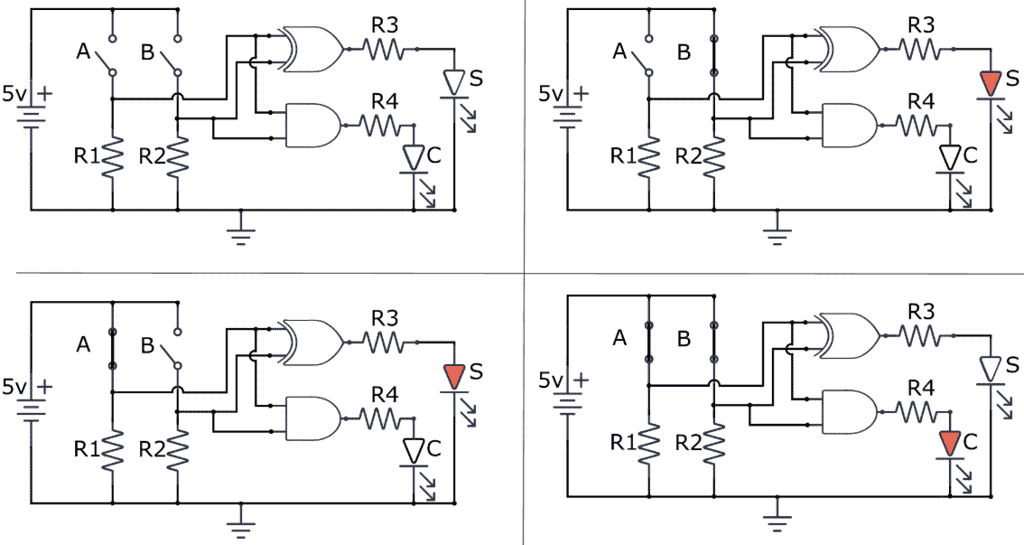
As a practical example, you can build an SR latch using the CD4001 chip. Below you can see how the CD4001 has four NOR gates inside, making it ideal for this kind of application.

The circuit works as follows: when the button PB2 is pushed, the LED L2 turns on and stays on even after PB2 is released, while the LED L1 remains off. LED L2 turns off when the button PB1 is pressed, whereas LED L1 turns and stays on even after PB1 has been released. To assemble the above circuit you need:
- The CD4001 chip
- Two push buttons (PB1 and PB2)
- Two LEDs
- Two 10 kΩ resistors (R1 and R2)
- Two 330 Ω resistors (R3 and R4)
Questions?
Do you have any questions about S-R Latch? Let me know in the comments below.
Copyright Build Electronic Circuits
Wednesday, 26 October 2022
Building with nanoparticles, from the bottom up
Printable circuits that can work on fabric, plastic and even fruit
Tuesday, 25 October 2022
Miniaturized infrared detectors
Wednesday, 19 October 2022
Blocking the buzz: MXene composite could eliminate electromagnetic interference by absorbing it
Tuesday, 18 October 2022
Halloween Electronics Project: Useless Machine
This year’s Halloween project is a useless machine built with 555 timers. It’s a coffin with a switch. When you flip it off, a dark force rises from the coffin and flips it back on.
Controlling a Servo with 555 Timers
The idea for this project came after we published the simple 555 PWM circuit that controls a DC motor using a PWM signal created by a 555 Timer. I started thinking about the idea of controlling a servo instead.
After some experimentation, I realized that the frequency changed too much when I changed the duty cycle. So my servo would only move at random times.
I decided to use two 555 timers instead: one in astable mode to set the frequency to a steady 50 Hz. And one in monostable mode that would set the duty cycle. With this setup, I was able to control the servo without any issues.
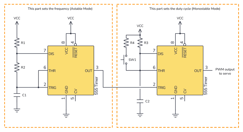
The value of the resistors R3 and the capacitor C2 sets the standard duty cycle. This position is when the arm is hidden.
When you push the pushbutton SW1, R4 is connected in parallel with R3 which reduces the duty cycle and moves the servo to its other position. This is the position that should make the arm flip off the toggle switch.
I used a pushbutton for this experiment. But in the useless machine setup, SW1 would be a toggle switch.
Adding a Delayed “button push”
The switching between the two positions happened a bit too fast. I was barely able to remove my finger before the servo arm moved into position to flip the switch back off. So I needed a way to delay things before the arm switched positions.
I tried a few different things before I ended up with the following: A pMOS to replace SW1. And a capacitor and resistor to add a delay from the toggle switch is flipped to the pMOS turns on.
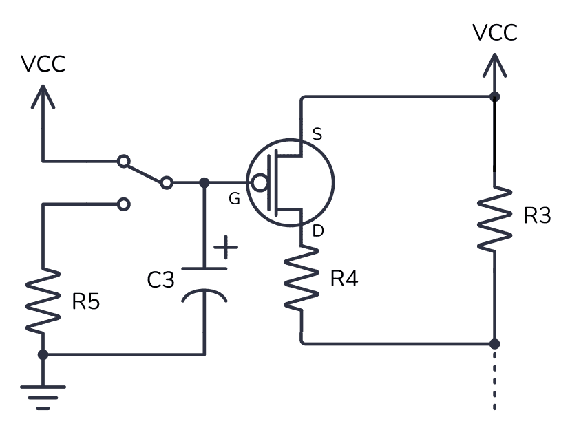
Basically, what this circuit does is that it places R4 in parallel with R3, just like SW1 did before. But it does so after a short delay of a couple of seconds. The values of C3 and R5 sets the delay time.
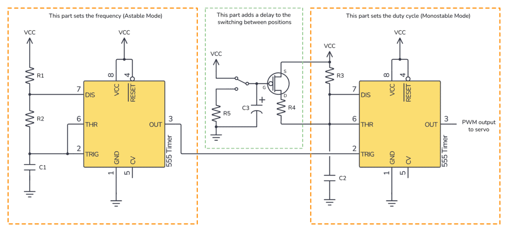
The Final Circuit
The delay circuit worked perfectly. And below you can see the full schematic for this project:
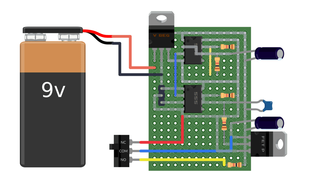
The only part of the circuit that is not shown above is a 7805 voltage regulator that converts my 9V battery to 5V, which was the VCC voltage I used to make everything compatible with my servo.
Components Needed
- 2 x 555 Timer
- 1 x pMOS transistor
- 5 x Resistors (See below for values)
- 3 x Capacitors (See below for values)
To choose values for the first 555 timer, use this 555 calculator in astable mode and try different values until you find the frequency you want.
Note that the time low you get will be the lowest possible duty cycle.
To choose values for the second 555 timer, use this 555 calculator in monostable mode and try different values until you find the resistance you need for the two different servo positions.
Use the highest resistance value for R3. Figure out what R4 needs to be in order to get the lowest resistance value (this calculator might be of help).
Copyright Build Electronic Circuits
Friday, 14 October 2022
Changing direction: Research team discovers switchable electronic chirality in an achiral Kagome superconductor
Smart materials: Metal cations-recognizable thermoresponsive polymers
Thursday, 13 October 2022
'Smart plastic' material is step forward toward soft, flexible robotics and electronics
Friday, 7 October 2022
Disposable electronics on a simple sheet of paper
Half Adder Circuit – How it Works
A Half Adder is a digital circuit that adds binary numbers. In this tutorial, you will learn how it works, its truth table, and how to implement one using logic gates.

What is a Half Adder?
A Half Adder is a digital circuit that carries out the addition of binary numbers. It’s the simplest of digital adders and you can build one using only two logic gates; an XOR gate and an AND gate.
The Half Adder can add only two 1-bit numbers. The difference between a Half Adder and a Full Adder is that the first one does not have a Carry input.
All the possible combinations of 1-bit binary additions are shown below:
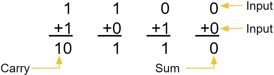
You need two bits to represent the result since the highest possible result of adding two 1-bit numbers is 2 (“10” in binary).
You can add this into a truth table using the four possible combinations of 1-bit binary additions given before. The adder takes two inputs, A and B, and generates two outputs, one for the Sum (S) and another for the Carry (C). So the truth table becomes:
| Input A | Input B | Output S | Output C |
|---|---|---|---|
| 0 | 0 | 0 | 0 |
| 0 | 1 | 1 | 0 |
| 1 | 0 | 1 | 0 |
| 1 | 1 | 0 | 1 |
How does the Half Adder work?
To understand how to create a Half Adder circuit you can use its truth table. The first thing you need to do is separate the S output and build its own truth table.
| Input A | Input B | Output S |
|---|---|---|
| 0 | 0 | 0 |
| 0 | 1 | 1 |
| 1 | 0 | 1 |
| 1 | 1 | 0 |
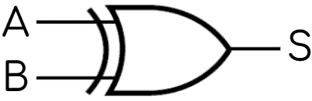
If you know your logic gates, you might notice that this looks exactly like the truth table of an XOR gate. And you’re right. So to implement the Sum (S) output, you’ll need an XOR gate:
Next, it’s time to focus on the C output:
| Input A | Input B | Output C |
|---|---|---|
| 0 | 0 | 0 |
| 0 | 1 | 0 |
| 1 | 0 | 0 |
| 1 | 1 | 1 |
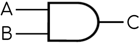
If you examine it carefully, you’ll see that it behaves the same as an AND gate since it only returns one when both inputs are one. This means that to create the C output you can use an AND gate:
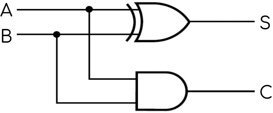
Finally, you can combine the circuits for producing the S and C outputs to build the complete Half Adder circuit diagram:
Half Adder simulation
To demonstrate this adder circuit works, you’ll find a simulation below. Simple switches represent the A and B inputs. The S and C outputs are represented by LEDs, where a lit LED means “1” and an unlit LED means “0”.
Questions?
Do you have any questions about how this adder circuit works? Let me know in the comments below.
Copyright Build Electronic Circuits
Thursday, 6 October 2022
Scientists develop inexpensive device that can harvest energy from a light breeze and store it as electricity
Wednesday, 5 October 2022
Phosphate's electrical signature helps detect important cellular events
Tuesday, 4 October 2022
Improving wearable medical sensors with ultrathin mesh
How to Build a Touch Sensor Circuit
In this project, you will build a touch sensor circuit. It’s a cool and simple circuit that allows you to control an LED with the touch of a finger. And you only need three components, how cool right?
You can build this circuit if you’re a total beginner.
The Touch Sensor Circuit Diagram
You only need a resistor, a transistor, and an LED to build this project. Below you’ll find the schematics for the touch sensor circuit:
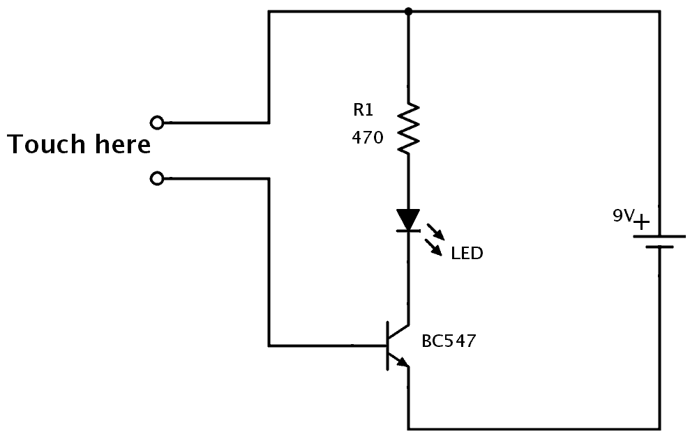
Components Needed
- 9V Battery
- 9V Battery Clip
- Breadboard
- Jumper Wires
- 470Ω Resistor
- Red LED
- NPN Transistor (BC546/547/548 or similar)
These are all standard components you can find at most electronics shops.
How It Works
Your body has electric resistance. You can check by measuring the resistance between your fingers with a multimeter.
So when you touch the wires of the touchpad, your body behaves as a resistor. This means a small amount of current can flow from the plus of the battery, through the transistor’s base, and turn on the transistor.
When the transistor is on, current can flow from collector to emitter of the transistor and the LED will turn on. Learn more about this in the article on how transistors work.
How to Build the Touch Sensor Circuit
You will build this circuit on a breadboard. But once you’ve tested that it works properly, feel free to go a step further and solder it.
Step 1: Connect The Transistor
Start by connecting the transistor a little bit down on the board.
If you’re using a BC546/BC547/BC548 transistor, you can connect it as shown in the figure. The collector goes into row 10, the base in row 11, and the emitter in row 12.
Note: If you have a different transistor model (ex the 2N3904), you need to check the datasheet to find out which leg is which, and adjust your connections accordingly.

Step 2: Connect The Resistor
Next, connect the resistor. Connect it from row 1 to row 9.
Notice that it is not connected to the transistor since the transistor is connected in row 10.
(In the following images, a 220 Ω resistor is shown. But it could be a good idea to use a larger value like a 470 Ω resistor to make sure your LED can handle the current.)

Step 3: Place The LED And Touchpad
Now, you’re going to connect the LED and the touch-sensing part. For the touch-sensing part, you’ll need two exposed wires. You can get this from the LED. The LED has much longer legs than needed.
Cut off the legs of the LED so that only around 1 cm / 0.4 in is left on the LED. Bend the two legs that you just cut off, as shown below, so that they fit in between four columns on a row.
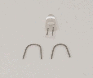
Place one on row 4 between column A and D. And one on row 6 between column A and D. This leaves room for a jumper wire to be connected later.
Insert the LED with its positive side on row 9 column F, and the other side on row 10 column F. Now the LED is connected between the resistor and the collector of the transistor, just like in the schematics of this circuit.

Step 4: Connect The Touchpad
Now you need to connect the two touch wires to the correct points in the circuit, using jumper wires.
Connect one jumper wire from row 1 column F to row 4 column E. And one jumper wire from row 6 column E to row 11 column I.

Step 5: Touch It!
Next, connect a jumper wire from row 1 column J to the positive supply column on the right. Then connect a jumper wire from row 12 column I to the negative supply column on the right.
Connect your battery connector and plug in the battery.

If everything is connected properly, nothing should happen right now.
But then, try to touch the touch wires so that your finger touches both wires at the same time, and the light will turn on.
If you can’t see the light, try making the tip of your finger wet before touching again. When the skin of your finger is wet, the resistance decreases so that more current can flow through your finger and to the base of the transistor.
What If There Is No Light?
In this circuit there are three common errors:
- the orientation of the LED is wrong
- the orientation of the transistor is wrong
- you are using a PNP transistor instead of an NPN transistor
- your finger is too dry
The NPN and the PNP transistors look exactly the same, so the only way to distinguish them is to look at what is written on the transistor. If it says BC557, it’s a PNP transistor, which is *not* correct. If it says BC546 (or BC547 or BC548) it’s NPN and it’s correct.
If you tried all of the above and it’s still not working, check the resistance value of your resistor. It should be 470 Ω. If it’s much more, it restricts the current to the LED too much. If it’s much less, it might have broken the LED.
If you have any questions about this experiment, use the comment field below.
The Result
In the video below you can see the process of building this, and the final result showing the working circuit:
Copyright Build Electronic Circuits
Monday, 3 October 2022
Stretchy, bio-inspired synaptic transistor can enhance, weaken device memories
Saturday, 1 October 2022
Exploring Jupiter's moon, Europa, possible with silicon-germanium transistor technology
-
CMOS (Complementary Metal Oxide Semiconductor) The main advantage of CMOS over NMOS and BIPOLAR technology is the much smaller power dis...
-
I was first introduced to logic gates when I was around 14 years old. I had heard that computers consisted of ones and zeroes. But I didn’t...
-
Do you need a MOSFET gate resistor? What value should it be? And should it go before or after the pulldown resistor? If you’re a bit impati...


