Saturday 28 August 2021

Highly conductive and elastic nanomembrane for skin electronics

Skin electronics require stretchable conductors that satisfy metal-like conductivity, high stretchability, ultrathin thickness, and ease of patternability, but it is challenging to achieve these characteristics simultaneously. The researchers developed a new float assembly method to fabricate a nanomembrane that satisfies all these requirements simultaneously. The exceptional material properties are attributed to its unique cross-sectional structure in which a monolayer of compactly assembled nanomaterials is partially embedded in an ultrathin elastomer membrane.

Thursday 26 August 2021

Research supports FDA recommendation: Patients with implanted medical devices should keep their smart phones and watches at least six inches away

A new study supports the FDA recommendation that patients keep any consumer electronic devices that may create magnetic interference, including cell phones and smart watches, at least six inches away from implanted medical devices, in particular pacemakers and cardiac defibrillators.

Promising candidates revealed for next-generation LED-based data communications

A new article has detailed how two relatively unexplored semiconducting materials can satisfy the telecommunication industry's hunger for enormous amounts of data at ever-greater speeds.

Engineers create double layer of borophene

Engineers have created a double layer of atomically flat borophene, a feat that defies the natural tendency of boron to form non-planar clusters beyond the single-atomic-layer limit.

New study unveils thermoelectric ink that turns car exhaust pipes into power generators

A recent study has resulted in the development of a thermoelectric technology method to produce power-generating tubes using 3D printing techniques.

Tuesday 24 August 2021

Discovery could improve reliability of future smart electronics

An undergraduate student has discovered a way to suppress hot-carrier effects that have plagued devices that use thin-film transistor architecture - such as smartwatches and solar panels.

Layered graphene with a twist displays unique quantum confinement in 2-D

Bilayer graphene with one of the two layers twisted displayed unique resonant electronic behavior. Understanding how electrons move in such 2-D materials could shed light on how to manipulate them for quantum computing and communication.

Monday 23 August 2021

Machine learning links material composition and performance in catalysts

In a finding that could help pave the way toward cleaner fuels and a more sustainable chemical industry, researchers have used machine learning to predict how the compositions of metal alloys and metal oxides affect their electronic structures.

Thursday 19 August 2021

Home-grown semiconductors for faster, smaller electronics

'Growing' electronic components directly onto a semiconductor block avoids messy, noisy oxidation scattering that slows and impedes electronic operation. A new study shows that the resulting high-mobility components are ideal candidates for high-frequency, ultra-small electronic devices, quantum dots, and for qubit applications in quantum computing.

Tuesday 17 August 2021

New method developed to solve plastics sustainability problem

A research group is developing polymers that can be broken down into their constituent parts; thus, when the catalyst for depolymerization is absent or removed, the polymers will be highly stable and their thermal and mechanical properties can be tuned to meet the needs of various applications.

Monday 16 August 2021

Heavily enriched: An energy-efficient way of enriching hydrogen isotopes in silicon

Deuterium, a heavier but less abundant version of the hydrogen atom, has many practical applications. Unfortunately, producing deuterium and using it to protect silicon-based semiconductors requires a lot of energy and very expensive deuterium gas. Now, scientists have discovered an energy-efficient exchange reaction to swap hydrogen atoms for deuterium on the surface of nanocrystalline silicon. Their results pave the way to more durable electronic devices while keeping costs and the environmental impact low.

Woven nanotube fibers turn heat energy into electrical energy

Carbon nanotubes woven into thread-like fibers and sewn into fabrics become a thermoelectric generator that can turn heat from the sun or other sources into other forms of energy.

Thursday 12 August 2021

Toward next-generation brain-computer interface systems

A new kind of neural interface system that coordinates the activity of hundreds of tiny brain sensors could one day deepen understanding of the brain and lead to new medical therapies.

Wednesday 11 August 2021

New electronic phenomenon discovered

Physics researchers at the University of North Florida's Atomic LEGO Lab discovered a new electronic phenomenon they call 'asymmetric ferroelectricity'. The research demonstrated this phenomenon for the first time in engineered two-dimensional crystals.

Friday 6 August 2021

New technology will allow important metals to be made more efficiently

Researchers have invented a cheaper, safer, and simpler technology that will allow a 'stubborn' group of metals, such as the Pt-group elements, to be transformed into thin films for various practical applications.

Thursday 5 August 2021

All in your head: Exploring human-body communications with binaural hearing aids

Wearable technology seems all poised to take over next-generation electronics, yet most wireless communication techniques are not up to the task. To tackle this issue, scientists have delved deep into human-body communications, in which human tissue is used as the transmission medium for electromagnetic signals. Their findings pave the way to more efficient and safer head-worn devices, such as binaural hearing aids and earphones.

Brain-inspired highly scalable neuromorphic hardware

Researchers fabricated a brain-inspired highly scalable neuromorphic hardware by co-integrating single transistor neurons and synapses. Using standard silicon complementary metal-oxide-semiconductor (CMOS) technology, the neuromorphic hardware is expected to reduce chip cost and simplify fabrication procedures.

Mixing a cocktail of topology and magnetism for future electronics

A new review throws the spotlight on heterostructures of topological insulators and magnetic materials, where the interplay of magnetism and topology can give rise to exotic quantum phenomena that are promising building blocks for future low-power electronics. Provided suitable candidate materials are found, a 'cocktail' of topological physics and magnetism could produce these key states at room temperature and without any magnetic field, making them a viable ultra-low energy alternative to current, CMOS electronics.

Tuesday 3 August 2021

Kick-starting supersonic waves in antiferromagnets

Researchers have demonstrated a new technique to generate magnetic waves in antiferromagnets that propagate through the material at a speed much larger than the speed of sound. These so-called spin waves produce a lot less heat than conventional electric currents, making them promising candidates for future electronic devices with significantly reduced power consumption.

MOSFET Gate Resistor

Do you need a MOSFET gate resistor? What value should it be? And should it go before or after the pulldown resistor?

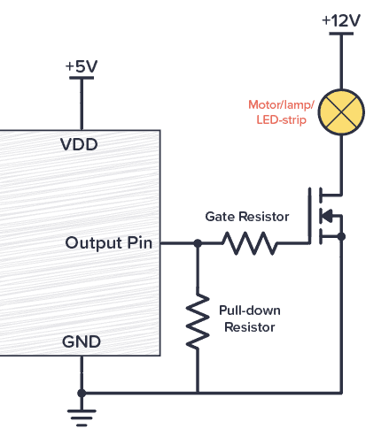
If you’re a bit impatient and just want the answer, here it is: You most likely need a gate resistor. And 1000 Ω will most likely work. See the circuit diagram below for connecting your MOSFET gate resistor (the Pull-down resistor is optional):

Mosfet gate resistor placement

Why Do You Need a Gate Resistor?

In how transistors work, we briefly touched upon that gate-to-source of a MOSFET acts as a capacitor.

Gate-source capacitor of a MOSFET

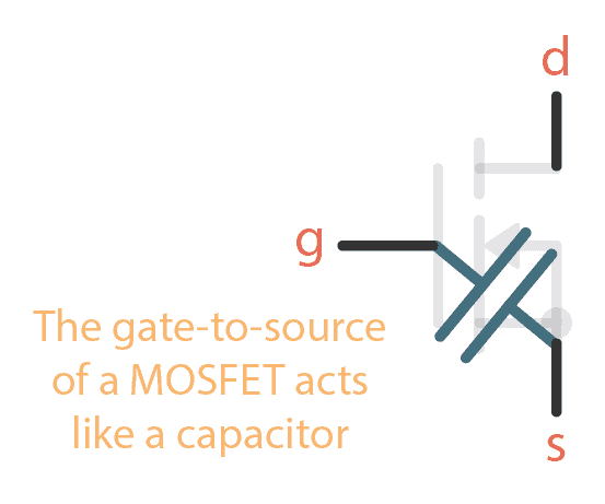
And a capacitor works like this:

  • When a capacitor is charging – current flows through it. A lot in the beginning, then less and less.
  • When a capacitor is fully charged – no current flows through it.

When your MOSFET is turned on, its gate-source capacitor is fully charged. So there is no current flowing through the gate.

But when your MOSFET is being turned on, you’ll have a current that is charging this gate-source capacitor. So for a small fraction of a second, there can be a lot of current flowing.

To make sure this short burst of current isn’t too high for your Arduino/Raspberry Pi/microcontroller (or whatever you’ve connected it to) you need to add a resistor in series between the output pin and the MOSFET transistor’s gate:

Arduino MOSFET transistor driver

Choosing A Resistor Value

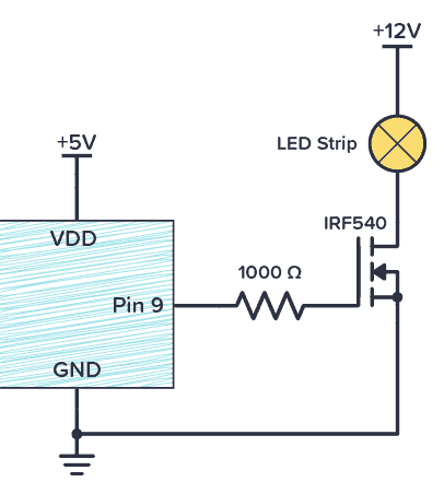
Often 1000 Ω is a good enough value for this. But it depends on your circuit.

You can calculate the maximum current you get from a resistor by using Ohm’s law for current:

I = \frac{V}{I}

For example in the case of Arduino that has 5V on its output pins, 1000 Ω gives you a maximum current of 5 mA (and Arduino pins can handle up to 40 mA):

I = \frac{5V}{1000 \Omega}

Keep in mind that the higher resistance you are using, the slower the MOSFET will turn on.

MOSFET Gate Resistor Placement

Are you using a pulldown resistor for your MOSFET? Then remember that if the gate resistor is placed to the left of the pulldown resistor, you get a voltage divider circuit that will reduce the voltage to the gate:

MOSFET pin driver circuit with pulldown (wrong placement)

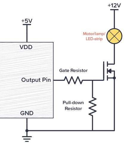
If you have chosen a gate resistor that is at least 100 times smaller than the pulldown resistor, then the reduction in voltage is so small that it doesn’t matter. But if they are a bit closer in value, the voltage on your gate will be lower than the pin voltage.

The solution? Switch places between the two so that the pulldown resistor is connected directly to the output pin:

Mosfet gate resistor correct placement

Copyright Build Electronic Circuits

New circuit boards can be repeatedly recycled

Researchers have developed a new PCB that performs on par with traditional materials and can be recycled repeatedly with negligible material...