Wednesday, 21 December 2022
At the edge of graphene-based electronics
Sunday, 18 December 2022
Wearable skin patch monitors hemoglobin in deep tissues
Friday, 16 December 2022
Researchers develop all-optical approach to pumping chip-based nanolasers
Thursday, 15 December 2022
A shield for 2D materials that adds vibrations to reduce vibration problems
Tuesday, 13 December 2022
The D Flip Flop (Quickstart Tutorial)
The D Flip Flop is an edge-triggered circuit that combines a pair of D latches to store one bit. It is commonly used as a basic building block in digital electronics to create counters or memory blocks such as shift registers.
In this tutorial, you will learn how it works, its truth table, and how to build one with logic gates.

What is a Flip Flop?
Latches and flip flops are sometimes grouped together since they both can store one bit (1 or 0) on their outputs. In contrast to latches, flip flops are synchronous circuits that need a clock signal (Clk). The D Flip Flop will only store a new value from the D input when the clock goes from 0 to 1 (rising edge) or 1 to 0 (falling edge).
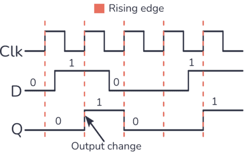
A D Flip Flop is built from two D latches. You can see a D Flip Flop that updates on the rising edge below:
The timing diagram for this circuit is shown below. It shows how a rising edge-triggered D Flip Flop behaves. The output Q only changes to the value the D input has at the moment the clock goes from 0 to 1.
How Does the D Flip Flop Work?
Since the output Q only changes when the Clock input goes from 0 to 1, you’ll get the following truth table:
| Clk | D | Q | Description |
|---|---|---|---|
| 0 | X | Q | Memory (no change) |
| 0→1 (↑) | 0 | 0 | Reset Q to 0 |
| 0→1 (↑) | 1 | 1 | Set Q to 1 |
| 1 | X | Q | Memory (no change) |
In the first and last rows of the truth table, the clock input is 0 and 1. None of them is a rising edge signal, so nothing happens. The Q output keeps whatever value it had. In this case, no matter what value the D input has, the Q output won’t change, it will keep its value as it is. This is how this circuit “remembers” a bit.
Have a look at the two middle rows. Here the clock input is going from 0 to 1, so you have a rising edge. This means that if the D input is 0, the Q output will be reset to 0. If the D input is 1, the Q output will be set to 1.
Presetting
D Flip Flops that you find in chips ready for use, such as the CD4013, usually also have Set and Reset inputs that you can use to force the D flip flop into starting with a 1 or a 0 on the output. Using these pins is sometimes referred to as “presetting” the D flip flop.
The Advantage of a D Flip Flop vs Latch

One of the downsides of the D latch is that its output can change at any time while its Enable pin is 1. So if you apply a clock signal to the D Latch, the Q output could also change during the time the positive pulse lasts.
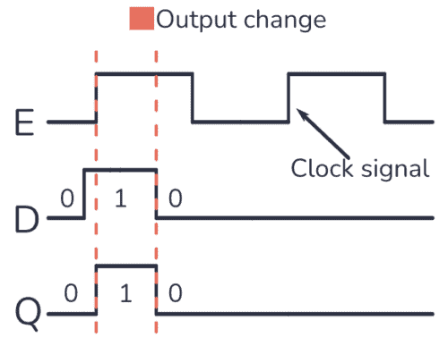
In the timing diagram above, you can see that during one clock cycle, the output is both 1 and 0 because the D input changes during the clock pulse. That’s something you don’t want to happen in a clocked digital system.
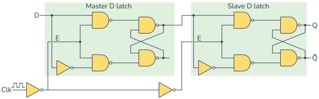
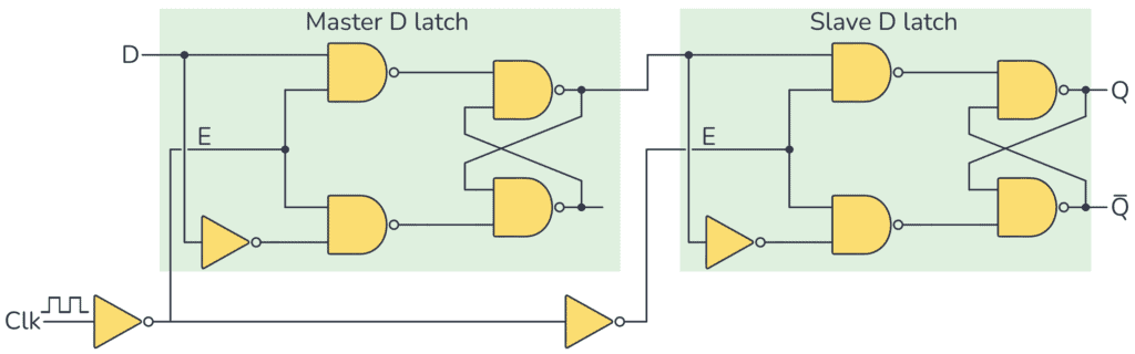
To get this flip flop to change its output only on the rising edges of the clock signal you can build a Master-Slave D Flip Flop Circuit, which requires a combination of two D latches as follows:

How It Works
The output from the master latch changes to what the D input has when the Clk input is 0.
If Clk is 0, it means that the Enable input of the slave latch is also 0. So nothing happens with the output of this latch.
But at the moment that Clk goes from 0 to 1 (rising edge), the Enable input of the slave latch is set to 1. That means whatever was on the output of the master latch at the moment Clk went from 0 to 1 is saved to the output of the slave latch.
If you substitute the symbols for D latches built with NAND gates you’ll get:
What Can You Use Them For?
The D Flip-flop is a very useful circuit. You can combine several D flip-flops to create for example shift registers and counters, which are used a lot in digital electronics. But you don’t have to build them from scratch. Instead, you can use the CD4013 chip that contains two D flip flops.
Shift Registers
To create a shift register, connect the output of one flip flop to the input of the next. New bits go into the first flip-flop on the left. And for every clock pulse, the bits stored in the other flip-flops are shifted one place to the right.
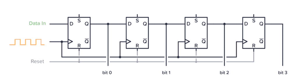
This is useful for example to get more output pins from an Arduino or other microcontroller. To control a shift register, you need one data pin and one clock pin. So with only two pins from the Arduino, you can control as many external pins as you want by using a shift register.
Ring Counters
If you take the output from the last flip-flop in a shift register and connect it to the input of the first flip-flop, you get a Ring Counter. Preset one of the flip-flops to start with 1, then this 1 will be shifted around and around in the Ring Counter.

The IC 4017 is a chip with this type of functionality, but with 10 outputs instead of just 4 like above. This makes for a fun chip you can use for example to create the Knight Rider LED bar.
Questions?
Do you have any questions about how the D Flip Flop works? Let me know in the comments below.
Copyright Build Electronic Circuits
The D Latch (Quickstart Tutorial)
The D Latch is a logic circuit most frequently used for storing data in digital systems. It is based on the S-R latch, but it doesn’t have an “undefined” or “invalid” state problem. In this tutorial, you will learn how it works, its truth table, and how to build one with logic gates.

What is a D Latch?
A D latch can store a bit value, either 1 or 0. When its Enable pin is HIGH, the value on the D pin will be stored on the Q output. It builds upon the design of the S-R latch, with a few added gates. You can see a D Latch circuit based on the S-R latch built with NAND gates below:

The inverter on the input makes sure the S and the R inputs are always opposites, to avoid the invalid state of both being 1. The two NAND gates create a new input, E (Enable), that lets you control when you want to change the output to whatever is on the D input.
This means that the output Q can only change when the enable signal is 1. If it’s 0, the output is unaffected by any changes on D.
You can also build a D Latch with AND and NOR gates as follows:

The D Latch can also be used to introduce delay in timing circuits, as a buffer, or for sampling data at specific intervals.
What’s the Difference Between Latch and Flip Flop?
The terms latch and flip flop are sometimes incorrectly used as synonyms since both can store a bit (1 or 0) at their outputs.
While a latch can change its output at any time as long as it’s enabled, a flip flop is an edge-triggered device that needs a clock transition to change its output.
To build a D Flip Flop, you’ll need two D latches, like this:

How Does the D Latch Work?
Since the output Q only changes when the E input is 1, you’ll get the following truth table:
| E | D | Q | Description |
|---|---|---|---|
| 0 | X | Q | Memory (no change) |
| 1 | 0 | 0 | Reset Q to 0 |
| 1 | 1 | 1 | Set Q to 1 |
In the first row of the truth table, the E input is 0. That means the latch is not enabled, so nothing happens. The Q output keeps whatever value it had. No matter what value the D input has, the Q output won’t change, it will keep its value as it is. This is how this circuit “remembers” a bit.
Take a look at the next two rows. Here the E input is 1, so the latch is enabled. This means that if the D input is 0, the Q output will be reset to 0. If the D input is 1, the Q output will be set to 1.
Analyzing the Circuit
You can build a D Latch circuit by adding three logic gates to the S-R latch circuit. In the next image, you can see the D Latch circuit’s bit path when it is enabled and it has 0 on the D input.

To analyze the above circuit you need to remember that the NAND gate only produces a 0 when its two inputs are both 1. In all other cases, it gives a 1.
To begin with, the inputs to the 1st NAND gate are 0 and 1, therefore, its output is 1. The 2nd NAND gate has both inputs at 1, so it returns 0.
The outputs of the 1st and 2nd NAND gates are the inputs to the section of the circuit that represents the basic S-R latch. With that in mind, you can divide the bits into two groups: Those that came before the S-R latch (Red) and those that were produced by the S-R Latch (Green).
Finally, if you look at the 4th NAND gate. You can see that one of its inputs is 0 due to the 2nd NAND gate. That information is enough to tell you that regardless of the value of its other input, it will give out 1. This bit is feedback to one of the inputs of the 3rd NAND gate. The other one is 1 due to the 1st NAND gate, so the result of the Q output is 0 – the same as input D.
Try going through this when D is 1 instead, and you’ll see that the output becomes 1.
From this bit path, you can conclude that the D Latch updates the output Q to what is on the D input as long as the E input is 1.
Experiment: Build Your Own D Latch Circuit
As a practical example, you can build a basic D Latch circuit using logic gates and test it out with pushbuttons. R1 and R2 are pull-down resistors to make sure the inputs are 0 when the buttons are not pushed:

As you can see in section 1 of the image, Q is 0 (LED L1 off), and both PB1 and PB2 are not pressed.
Next, look at section 2 where PB2 is pushed. You now have a 1 on the D input, but the output Q remains as 0 because the E input hasn’t received an enable signal yet.
Section 3 shows how PB1 is pressed, so a 1 on the E input appears and places the bit 1 from D to Q. When Q is 1 it turns on LED L1.
When PB1 and PB2 return to their original states in section 4, LED L1 remains ON indicating that the Q output has not changed.
To change the output Q you would need to push PB1 again.
To assemble the above circuit you need:
- Four NAND gates (Ex CD4011)
- One NOT gate (Ex CD4049 or CD4069)
- 2x pushbuttons
- 1x LED
- 2x 10 kΩ resistors (R1 and R2)
- 1x 330 Ω resistors (R3)
Copyright Build Electronic Circuits
Sunday, 11 December 2022
Paper-thin solar cell can turn any surface into a power source
Recycled gold from SIM cards could help make drugs more sustainable
Saturday, 10 December 2022
Molecules have an orientation, and scientists have a new way to measure it
Thursday, 8 December 2022
Solving the puzzle: Cubic silicon carbide wafer demonstrates high thermal conductivity, second only to diamond
Wednesday, 7 December 2022
Flameproofing lithium-ion batteries with salt
-
Bluetooth Controlled Electronic Home Appliances is a simple project, where we can control different electrical appliances and electronic de...
-
CMOS (Complementary Metal Oxide Semiconductor) The main advantage of CMOS over NMOS and BIPOLAR technology is the much smaller power dis...
-
I was first introduced to logic gates when I was around 14 years old. I had heard that computers consisted of ones and zeroes. But I didn’t...


