Gerber files are actually images of the different layers of your Printed Circuit Board (PCB). And it’s a universal way of sending your design to a PCB manufacturer. In this tutorial, I’ll show you how to create these files in KiCad.
How Gerber Files Work
Gerber files use the Gerber format.
When you design a PCB in KiCad (or any other software), you are drawing different layers. For example, the copper on top of your board is drawn in one layer. And the top silk print is drawn in another layer.
Each Gerber file represents only one of these PCB layers. That means you will usually get seven files for a two-layer board:
- Board Outline
- Top Copper Layer
- Bottom Copper Layer
- Solder Stop Mask
- Solder Stop Mask
- Silk Top
- Silk Bottom
If you want to create a stencil for solder paste, you also need the solder paste layers.
Drill Files
For some reason, it’s normal to use the Excellon file format to create drill files. That’s why you have to create a drill file in addition to the files above.
Creating Gerber Files in KiCad
Start by opening your KiCad design in the Pcbnew (the PCB Editor of KiCad).
Then go to the File menu and select Plot…
A window will pop up.
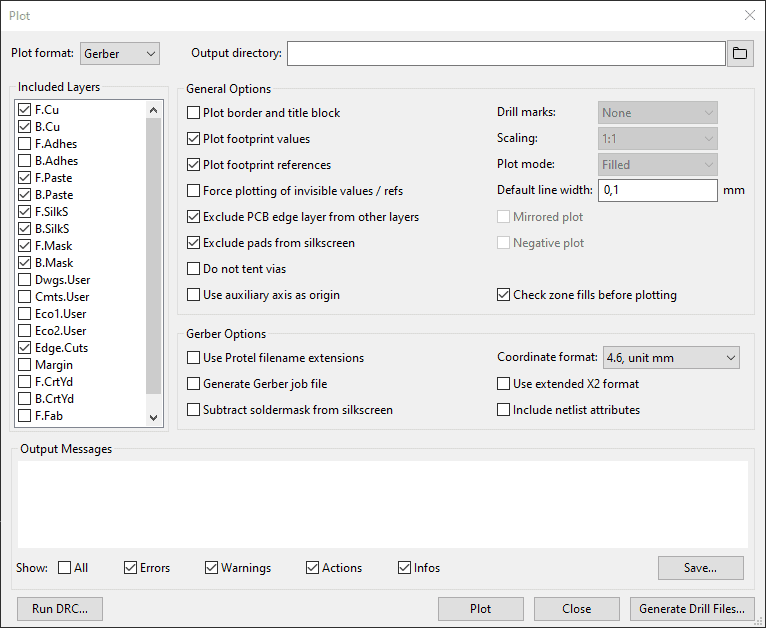
Select the layers you want to include. Then click on the Plot button to create the Gerber files. If you leave the Output directory field empty, the files will be saved in the same folder as your project files.
Creating Drill Files in KiCad
To create Drill files, click on Generate Drill Files… to open the Drill File dialog.
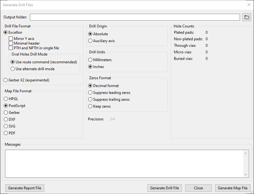
You can usually leave the default options. Then click the button Generate Drill File. In the Messages field, you’ll see a message with the filename of the generated file. It should have a .drl ending.
Instructions For Specific Manufacturers
There are a lot of options when generating these files. Often the PCB manufacturer you want to use will have instructions on what options to choose.
Questions?
Are you struggling with Gerber files? Or are any of the instructions above unclear?
Let me know in the comment field below!
Copyright Build Electronic Circuits


No comments:
Post a Comment